Schottky Field Emission Sources
A single crystal tungsten wire with a sharp end etched to a small radius (red in the sketch) is mounted on a tungsten hairpin (also red). A current through the filament is used to maintain the tip at a temperature of 1750 - 1850 K. The tip just penetrates a hole in a cylindrical suppressor electrode mounted around the assembly. Electrons are emitted from the tip due to both thermal excitation and the electric field at the tip due to the potential difference between it and an extractor electrode (not shown). Electrons from the filament are repelled by the potential on the suppressor. Electrons from the tip are used by the subsequent column to form a focussed beam.

Details are given in: Swanson and Martin. Journal of Applied Physics, 44, 2029-2050, 1975; and Wolfe - Journal of Vacuum Science and Technology, 16, 1704-1708, 1979
YPS SCHOTTKY TIP
SEM image of a YPS Schottky tip. Emission occurs from the crystalline facet (vertical at the right-hand end) that is about 0.1-5μm across.

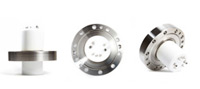
Re-tipping of Schottky and field emitter packages
There are situations where a need to re-tip a specific or out of production field emitter or Schottky field emitter is needed. YPS is able to offer such a service, depending on the specific case under discussion. Examples of such a service include but not restricted to; re-tipping of the mini-module source used on Applied Materials CD SEMs, some early field emission based electron columns.